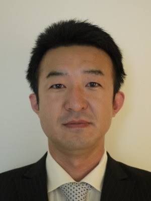
Masayoshi Tagami -- Invited Speaker, 3DIC 2026
CMOS Directly Bonded to Array (CBA) Technology for Future 3D Flash Memory
Abstract
This work investigates CMOS direct-bonded-to-array (CBA) technology for 3D flash memory and demonstrates a multi-stacked-array CBA (MSA-CBA) technology with quad-level-cell (QLC) operation. A novel alignment-correction technique for the wafer-to-wafer copper direct-bonding process mitigates bonding opens caused by misalignment due to saddle-shaped wafer warpage during multi-array stacking. The technique improves the daisy-chain yield for bonding pads with sub-800-nm pitches. Electromigration, stress-induced voiding, and package reliability all meet the target specifications. A prototype MSA-CBA device demonstrates QLC operation and the feasibility of mitigating cell-current degradation, wafer warpage, and challenges associated with large block sizes, thereby advancing ultra-high-density 3D flash-memory technology.
Biography
Masayoshi Tagami received the B.E. and M.E. degrees from Tokyo Institute of Technology (now Institute of Science Tokyo) in 1996 and 1998, respectively, and the Ph.D. degree in electrical engineering from Tohoku University in 2015. He joined NEC Corporation in 1998, where he was engaged in research and development on back-end-of-line (BEOL) process integration for logic LSIs. In 2013, he joined Toshiba Corporation (now Kioxia Corporation), where he has been engaged in research and development on BEOL and 3DIC processes integration for 3D flash memory. He is currently a Group Manager of the Advanced Memory Research and Development Group. He has presented his work at several international conferences and serves as a committee member of the IEEE International Interconnect Technology Conference (IITC).